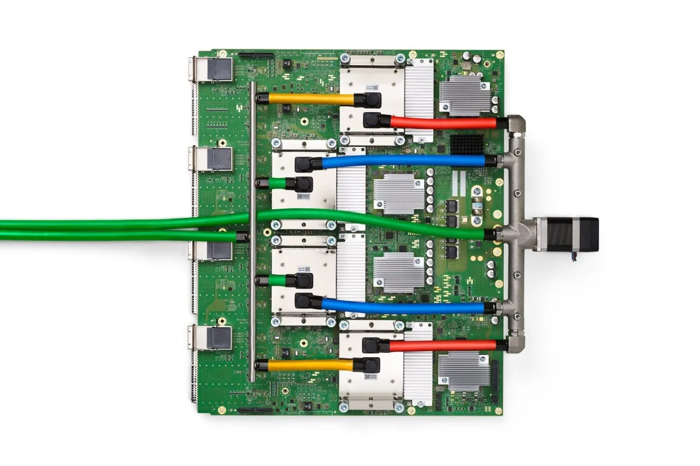
A TPU, or tensor processing unit, is the custom chip Google designed to run the math behind its AI services, and the reported next-generation design effort with AMD has kept the hardware in the headlines. This guide explains what a TPU actually is, how TPUs vs GPUs compare for training and inference, who builds these chips, and what access costs.
What is a TPU?
In computing, a TPU (tensor processing unit) is an application-specific integrated circuit built for one job: the tensor, or matrix, operations behind neural networks. Google designs TPUs in-house and deploys them in its own datacenters, where they train and serve models such as Gemini. The company’s research team introduced the design in a 2017 paper covering chips that had already been running production inference workloads since 2015.
The acronym has other meanings outside computing: thermoplastic polyurethane shows up in phone cases, watch straps, and 3D printer filament. This article is about the chip. When shoppers search for a TPU case or TPU filament, they are in a different aisle entirely.
TPU vs GPU: what’s the difference?
A GPU is a general-purpose parallel processor: thousands of cores that render game graphics and, as it turned out, accelerate almost any AI framework on the market. NVIDIA dominates merchant AI hardware because its GPUs are flexible, widely available, and supported everywhere. A TPU trades that flexibility for focus. It runs a narrower slice of computation, the matrix multiplies that dominate neural-network work, and Google tunes the entire system around that workload, which is where its efficiency gains come from.
That split explains who uses which. Any developer can rent a GPU by the hour from a long list of clouds and vendors. TPUs are available only through Google Cloud, so organizations that want them are effectively buying into Google’s stack. In performance-per-watt on the workloads it targets, Google argues its approach wins; in breadth of ecosystem, the GPU still defines the market.
TPU vs GPU vs CPU
The three engines divide the work differently. A CPU handles general-purpose logic, operating systems, and application code with a few powerful cores. A GPU brings massive parallelism to graphics and AI math. A TPU narrows further, to tensor operations, and sits inside clusters built specifically for machine learning. Modern PCs add a fourth engine, the NPU, for power-efficient on-device AI; our NPU vs GPU vs CPU explainer covers that comparison in depth.
How does a TPU work?
The heart of a TPU is a large matrix multiply unit organized as a systolic array, a grid of multiply-accumulate cells that pushes data through in rhythmic waves so values are read from memory once and reused across many calculations. The original chip packed a 256×256 array of 8-bit multiply-accumulate units, a design choice the Google engineers’ 2017 analysis credits with large gains in operations per second per watt over contemporary CPUs and GPUs on neural-network inference.
Scale comes from the network around the chip, not just the die. Later generations connected thousands of TPUs into pods over high-speed dedicated interconnects; the TPU v4 paper describes an optically reconfigurable supercomputer that rewires those links between pods as workloads demand. That system-level view, chips plus interconnect plus software co-designed together, is what separates a TPU fleet from a pile of accelerators.
Who makes TPU chips?
Google owns the TPU architecture and leads the system design. Broadcom has been a co-development partner, translating Google’s specifications into manufacturable ASIC designs, while TSMC is the foundry reported to fabricate the silicon for that partner mix. TrendForce’s reporting describes that division of responsibility while noting that the partner mix can change by generation.
The newest name in the story is AMD. A SemiAnalysis client note cited by Tom’s Hardware reports that Google is working with AMD on a TPU project in the tenth generation, one that would place general-purpose CPU cores on the same package as the tensor compute. The rationale is workload-driven: reinforcement learning and agentic AI hammer the CPU side of the house, and Google’s own inference-oriented systems have already been increasing the ratio of CPUs to accelerators. For AMD, the project would be a first major role in someone else’s custom AI accelerator. Neither Google nor AMD has confirmed the report or commented publicly, so every detail remains a directional signal rather than a product announcement.
Google’s chips are one species of a wider genus. An AI accelerator chip is any processor built specifically for neural-network math, a group that includes Google’s TPUs, NVIDIA’s datacenter GPUs, AWS Trainium, Microsoft Maia, and Meta’s MTIA, plus startup silicon from Groq and Cerebras. The common thread is specialization: each trades general-purpose flexibility for efficiency on AI workloads.
Google TPU generations
Google’s TPU family has moved from inference-only v1 to training-capable pods, optically linked v4 systems, and specialized current chips. The lineage below is a compact guide to major generations, with dates and names based on Google’s published announcements and research papers rather than every interim variant.
| Generation | First shipped | Notable for |
|---|---|---|
| TPU v1 | 2015 | Inference-only original, revealed publicly in 2016 |
| TPU v2 / v3 | 2017 / 2018 | Training support, pod-scale clustering |
| TPU v4 | 2021 | Optical circuit switches rewire pod interconnects |
| TPU v5e / v5p | 2023 | Cost-efficient inference and largest training pods |
| Trillium (v6e) | 2024 | Sixth generation, big jump in throughput per chip |
| Ironwood (seventh gen) | 2025 | First TPU designed for inference at scale, generally available November 2025 |
| Eighth generation | Announced April 2026 | Two chips: TPU 8t for training, TPU 8i for inference; availability later this year |
Google announced the eighth-generation pair at Cloud Next as purpose-built silicon for agentic workloads, with the training chip targeting nearly three times the compute per pod of Ironwood and the inference chip targeting 80 percent better price-performance than its predecessor. The company’s announcement covers both chips, and Ironwood’s own rollout is documented in the seventh-generation reveal.
Why AI datacenters are looking past copper
A TPU rack is only as fast as the links between its chips, and that layer is being rebuilt. As clusters scale, copper interconnects hit limits in reach, density, and energy per bit, which is why optical approaches keep advancing. Avicena, a Sunnyvale startup, has begun shipping evaluation kits for a laser-free microLED-based link that carries up to 1 Tbps over fiber bundles aimed at exactly these die-to-die and XPU-to-XPU connections; we covered the Avicena LightBundle shipment separately. Expect the wiring inside future accelerator racks, Google’s and everyone else’s, to look less like cabling and more like photonics.
Can you buy a TPU? TPUs vs GPUs for your AI projects
No retail channel exists: Google builds TPUs for its own datacenters and rents capacity rather than selling chips. Access runs through Google Cloud’s TPU service, billed per hour by chip type, with current rates published on Google’s pricing pages rather than fixed list prices, because cloud pricing changes often enough that any snapshot here would rot. For anyone building locally, the practical answer to the TPU-vs-GPU question is a GPU: it plugs into a workstation, runs every framework, and needs no cloud contract. Our coverage of desktop AI hardware follows the same logic.
There is one free on-ramp. Google’s Colab notebooks include complimentary TPU runtime access alongside GPUs for quick experiments, subject to availability limits documented in the Colab FAQ. It is the closest thing to trying a TPU without a billing account.
Prefer your hardware explainers closer to the desk? We also track what ships in it, from Intel’s Nova Lake roadmap to budget GPU picks.
TPU FAQ
What does TPU stand for?
Tensor processing unit. A tensor is the multidimensional array format that neural networks use to represent data, and the chip is purpose-built to multiply those arrays at scale.
Is a TPU better than a GPU?
Better depends on the job. On the tensor-heavy workloads it targets, a TPU can deliver more performance per watt, which is why Google runs its own services on them. GPUs win on availability, flexibility, and ecosystem: they are sold by many vendors, run everywhere, and remain the default choice for local and merchant AI compute.
Who makes TPU chips for Google?
Google designs them, Broadcom co-develops the ASIC designs, and TSMC fabricates the silicon. Reporting in 2026 added a possible second collaborator: a SemiAnalysis note cited by Tom’s Hardware describes AMD working with Google on a tenth-generation variant with on-package CPU cores, a report neither company has confirmed.
Does AMD make TPUs?
Not today. AMD sells its own Instinct accelerators and, according to the unconfirmed report above, may contribute CPU cores and packaging expertise to a future Google design. If it happens, it would be AMD’s first role in another company’s flagship custom AI chip, but nothing has been announced.
TPUs matter because they mark the industry’s path: special-purpose silicon, co-designed with the software it runs, replacing general-purpose chips wherever a workload is predictable at scale. Watch this page as the eighth-generation chips reach customers; every new fact about Google’s accelerator roadmap lands right here.