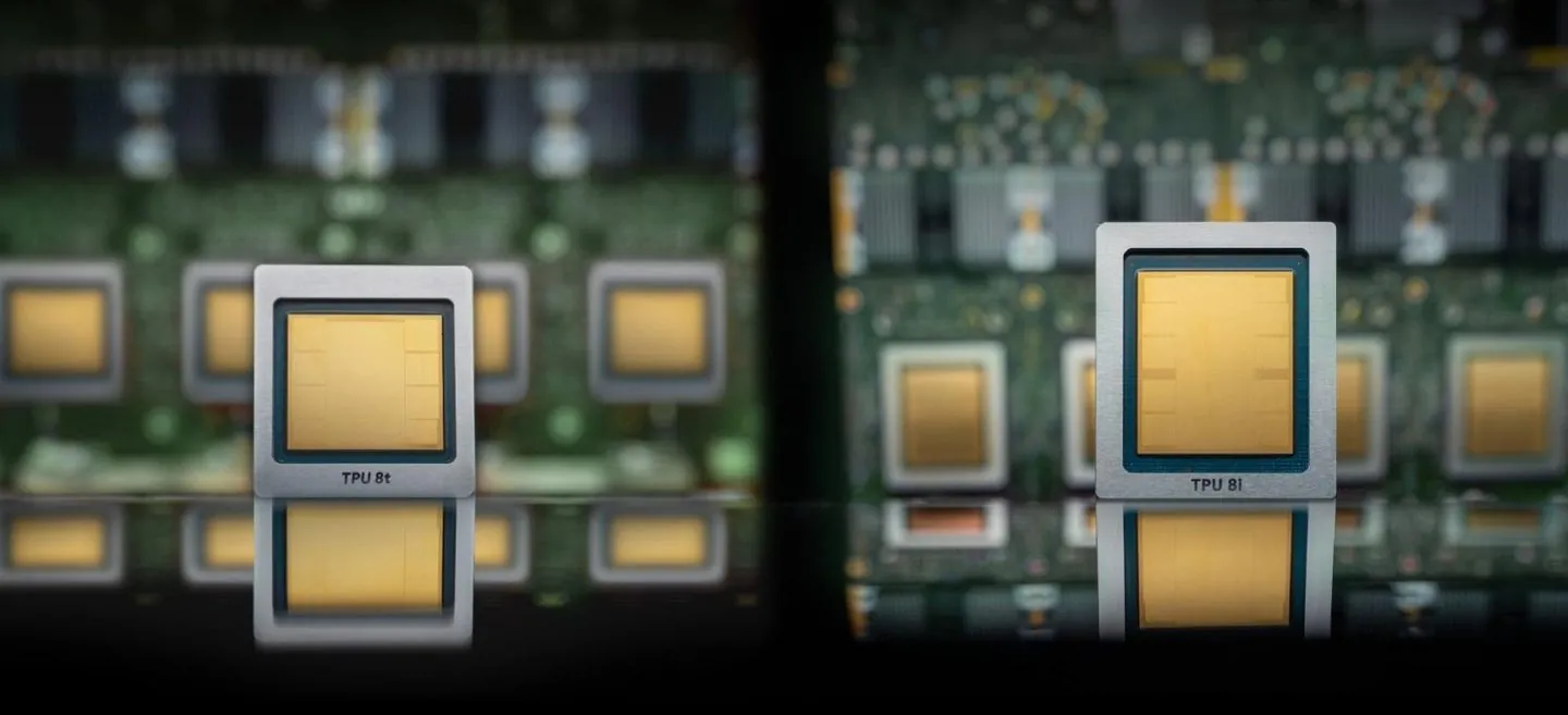
Google used this week’s Hot Chips 2026 conference to pull back the curtain on the internals of its eighth-generation Tensor Processing Unit, and the headline is a clean split: for the first time the TPU family ships as two separate chips, one for training and one for serving. The TPU 8t targets massive pre-training, while the TPU 8i is built for low-latency inference and reinforcement learning. Google’s Cloud blog first named the pair at Cloud Next in April, but the Hot Chips disclosure added the architectural detail behind the decision. Google’s technical deep dive frames the split as a response to the operational demands of agentic AI.
The reasoning is that training and serving have drifted into different bottlenecks. Mixture-of-experts models push far more traffic across the system than older dense models, and agentic workloads punish latency as a chain of tool calls and state saves stretches out. One architecture cannot serve both roles efficiently, Google argues, so the two chips optimize for different memory, networking, and latency profiles. The inference chip carries more high-bandwidth memory per unit of compute and a higher share of on-chip SRAM, while the training chip leans into raw FLOPs and interconnect.
The training superpod and the inference node
On the training side, the TPU 8t scales to 9,600 chips in a single superpod with 2 petabytes of shared HBM and 121 exaflops of FP4 compute, about twice the performance per watt of the prior Ironwood generation. Google also introduced the Virgo network fabric for 8t, linking more than 134,000 chips in one domain at up to 47 petabits per second of bi-sectional bandwidth. On the inference side, the TPU 8i is notable for pairing two of Google’s in-house Axion Arm CPUs with each chip node, replacing the x86 hosts used in earlier inference systems and moving Google fully onto its own Arm-based silicon for serving.
The 8i also changes its network shape. Where training used a 3D torus, the inference chip uses a lower-latency fly topology with a maximum of seven hops versus sixteen on the torus, and it performs in-network collectives on the I/O die next to the networking hardware rather than dragging data back to the compute die. As we explained in our TPU vs GPU guide, inference is memory-bandwidth bound, so moving collectives off the compute path is exactly where an inference-specialized part earns its keep.
Axion, co-design, and the agentic bet
Google says existing TPU code runs on the v8 family, and developers who want the most can drop to Pallas, its Python kernel language inside JAX, to write hardware-aware kernels. The company also reports using its own AI models during 8t development to trim power and recover die area for more compute cores, extending a co-design habit it has leaned on across seven prior generations. The same Hot Chips week also surfaced OpenAI’s first inference-chip benchmarks, a sign that the race to own the serving layer is now a silicon race among the model labs themselves.
Neither chip has a precise general-availability date beyond “later in 2026” for Cloud customers. The practical question is whether customers port frontier models to TPUs at scale, something Google has pushed for with Anthropic as an anchor tenant. If the split design delivers the latency and efficiency it claims, it gives Google a distinct position: the only hyperscaler building purpose-built silicon for both training and inference in the same generation, rather than buying commodity hardware for one and designing the other. Our coverage of rising AI server prices shows why controlling that stack now matters for the 2027 capital budgets of every major operator.