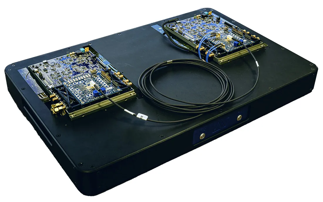
Avicena has begun shipping 1 Tbps LightBundle evaluation kits, moving its microLED-based optical interconnect from a conference demonstration to working hardware in customer laboratories. The Sunnyvale company announced the milestone on August 18 in a release distributed through HPCwire, after first showing the kit at the Optical Fiber Conference (OFC26) in March.
The evaluation kit pairs a 335-channel microLED array, with each channel operating at up to 3 Gbps, with a multicore fiber bundle that carries the light to a 335-element integrated photodiode array. Avicena says the channels together provide up to 1 Tbps of aggregate raw throughput, built on what it calls a laser-free optical architecture that targets low power, high bandwidth density, reliable operation at elevated temperatures, and reach beyond the practical limits of copper.
Why AI systems are looking past copper
AI systems are raising the bandwidth demanded between accelerators, memory, and switch fabrics, and link rates keep climbing. Copper interconnects face growing challenges in reach, routing density, and energy efficiency at those rates, while conventional optics built around lasers and silicon photonics extend reach but bring power, bandwidth density, cost, and reliability challenges of their own. Avicena’s approach replaces the laser with dense microLED transmitter arrays coupled through fiber to photodetector arrays, an architecture designed to run across demanding system temperatures. The target connections are the ones closest to the compute: die-to-die, die-to-memory, XPU-to-XPU, and XPU-to-switch, the same fabric where memory bandwidth has become the constraint on AI performance.
The kit gives engineering teams a complete platform for evaluating link behavior in their own laboratories. Host interface boards, integrated diagnostics, and a graphical user interface support characterization of optical signal integrity, link budgets, eye quality, crosstalk, power efficiency, and bit error rate.
What the shipment means
“Shipping our 1 Tbps LightBundle eKits extends Avicena’s microLED-based optical interconnect leadership and represents a significant milestone in delivering the terabit-class connectivity required to scale next-generation AI infrastructure,” said Marco Chisari, CEO of Avicena, in the release. Analyst Bob Wheeler of LightCounting called the shipment “a meaningful milestone for the optical-interconnect industry,” noting that a practical terabit-class platform lets developers evaluate microLED technology for XPU-to-XPU, XPU-to-memory, and XPU-to-switch links as the technology advances toward production.
The platform is aimed at both directions AI systems scale. Scale-in links connect accelerators and memory tightly inside a node, while scale-up links carry traffic across accelerators and into the switch fabric, and Avicena positions the same microLED architecture for both. The company is a privately held startup headquartered in Sunnyvale, California, and it describes the laser-free approach as the basis for reliable, scalable optical connectivity across the next generation of AI systems.
The eKits are shipping now to customers and partners building AI infrastructure, and Avicena is taking integration inquiries directly. Evaluation availability is the next stage on the road to production: the market will answer with these kits whether microLED optical links hold up inside real accelerator and memory subsystems, and at what power per bit. For buyers, the practical result is that the interconnect layer is becoming a design decision in its own right, alongside the power and bandwidth budgets that already shape AI hardware choices.