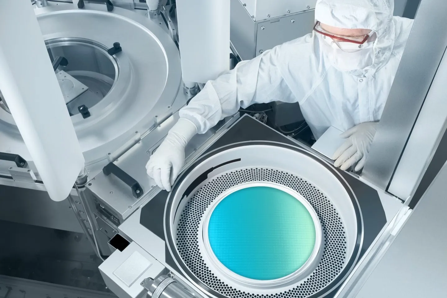
Lam Research (NASDAQ: LRCX) said on August 13 that it plans to invest more than $3 billion over the next five years to expand its global research and development lab network, a move the wafer fabrication equipment maker says will lift its experiment capacity by more than 50 percent as chipmakers chase AI-era designs. The company announced the multi-site expansion in a press release outlining a network of specialized labs across the United States, Asia, and Europe that already supports more than one million experiments annually.
Lam builds the deposition, etch, and strip tools used to pattern advanced chips, and its R&D organization is one of the biggest in the equipment industry. The company said the expansion will add infrastructure and capabilities at multiple sites, with work starting this year. Its labs operate as an integrated 24/7 network, and Lam says the goal is to compress product development cycles for customers from pathfinding to fab deployment, with process development shortened up to 2.5 times in recent customer engagements.
Why equipment R&D is scaling up
The investment is a direct response to the same pressure we have tracked in the chip race becoming a power race: AI accelerators need new architectures, new materials, and features engineered at nanoscale precision, and every one of those changes lands first in the fab, where etch and deposition tools decide what is physically possible. Lam’s CEO Tim Archer framed it that way in the announcement. “In the AI era, the pace of innovation is relentless, requiring chips with new architectures, different materials, and complex features engineered with nanoscale precision,” he said. “Our ability to increase velocity throughout the R&D process has become a decisive advantage.”
The company runs specialized facilities for foundational research in new chemistries, materials, and mechatronics, and says those labs can compress weeks of experimental work into as little as a few days. Process development labs then carry results toward production readiness with engineering and manufacturing teams working on the same tools, and technology centers located near customers handle rapid qualification and validation. Tools, data, and expertise are shared across time zones, so a discovery in one lab becomes available to every lab in the network.
The announcement drew support from a customer and an industry analyst. Micron’s executive vice president and chief technology and products officer Scott DeBoer said the memory maker’s collaboration with Lam continues to drive innovation in leading-edge front-end and advanced packaging technologies. John West, chief analyst for semiconductor equipment at Yole Group, said AI-related investment is lifting demand for deposition and etch intensity, and that sustaining the momentum will require the ecosystem to innovate faster and scale new technologies into manufacturing more quickly.
What the money buys
Lam did not break down the $3 billion by site, but the press release says the planned expansion is expected to add infrastructure and capabilities to increase experiment capacity by more than 50 percent. The lab network already spans the United States, Asia, and Europe, and the company’s equipment is used in nearly every advanced chip built today. The five-year timeframe lines up with the industry’s current buildout cycle, in which foundries, memory makers, and logic manufacturers are all adding capacity for AI silicon.
The investment is part of a broader pattern across the semiconductor supply chain. As we noted in our coverage of memory bandwidth becoming the new bottleneck in AI hardware, the pressure on fabs is coming from every direction, and equipment makers are scaling their own R&D to keep pace. The announcement also follows a wave of capital deployment up and down the industry, from Nvidia’s $500 billion compute financing plans to memory vendors pushing new storage architectures for AI workloads.
Lam frames the expansion as a way to stay ahead of what customers need. “We are investing with the intention of staying ahead of what our customers need, further strengthening our global innovation engine to deliver the next generation of semiconductor breakthroughs,” Archer said. The company plans to begin expanding the lab network this year, with the stated goal of increasing innovation velocity as the AI cycle drives demand for more capable chipmaking tools.