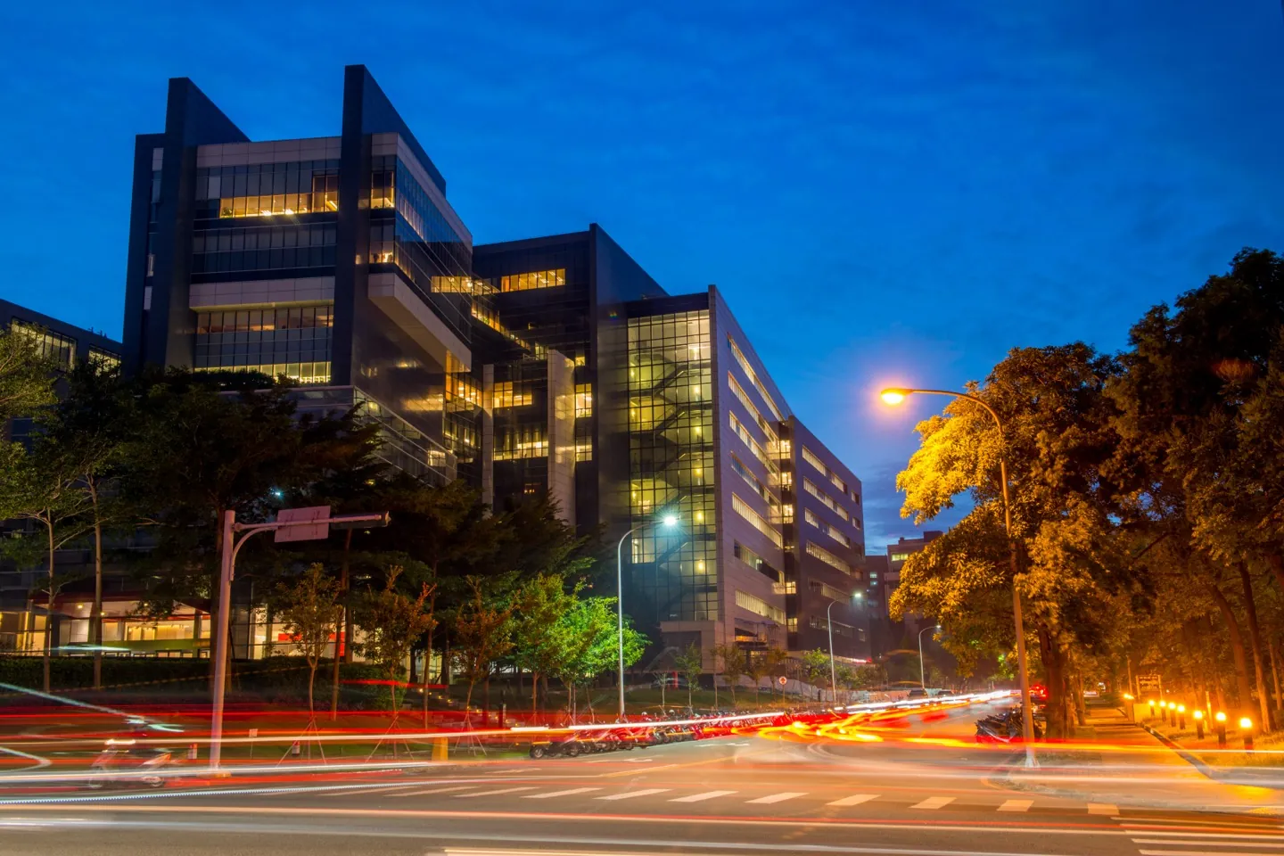
Sony Semiconductor Solutions and TSMC have signed a legally binding agreement to establish Advanced Vision Semiconductor Manufacturing Corporation, a joint venture in Koshi City, Kumamoto Prefecture, that will develop and produce image sensors for smartphones using advanced process technology, TSMC announced on August 11. Volume production is expected to begin in 2029, and the JV is planned to operate as a consolidated subsidiary of Sony Group.
Sony will be the sole controlling shareholder, and Sony will appoint the JV’s representative director. Under the deal, Sony plans to contribute approximately 465 billion yen through a combination of cash and the transfer of its newly constructed fab in Koshi City, where it has already invested, via a company split. TSMC plans to make cash contributions of approximately 282 billion yen. The combined contributions, roughly 747 billion yen, are expected to be made in phases based on market demand and business conditions, and investments needed to reach the JV’s planned production capacity are being considered on the premise of support from the Japanese government.
Why Sony keeps TSMC close
Sony will take the lead on core image sensor technology, product planning and product design, while the JV leverages TSMC’s advanced process technology and manufacturing expertise for volume production. The two companies describe the split as a way to accelerate commercialization of customer-driven image sensor products while strengthening manufacturing capacity. The agreement follows the preliminary agreement the companies announced on May 8, 2026, and the establishment of the JV still requires regulatory approvals and other customary closing conditions.
The deal consolidates a relationship that has been building for years. Sony Semiconductor Solutions already holds a stake in JASM, TSMC’s first Japan fab in Kumamoto, and this new JV extends the partnership from logic wafers into a dedicated image sensor production line. Image sensors are Sony’s core semiconductor business, and the company has long dominated the smartphone camera sensor market, but it has relied on external foundries for advanced process capacity. TSMC brings the leading-edge manufacturing that image sensors increasingly need as smartphone cameras push toward larger sensors, higher resolutions and stacked designs that pair logic and pixel layers.
The location matters as much as the technology. Kumamoto Prefecture has become the center of TSMC’s Japan expansion, and the region is assembling a semiconductor supply chain around JASM and its suppliers. A dedicated Sony-TSMC sensor line in the same region shortens the supply chain for Sony’s sensor business, which already operates a technology center in Kumamoto. The yen-denominated contributions and the expected Japanese government support also signal that both companies are betting on Japan as a manufacturing base for the next generation of camera hardware.
The 2029 timeline puts the JV at the center of the industry’s transition to bigger smartphone camera systems. Sony’s sensor roadmap has been pushing pixel counts and sensor size upward, and stacked CMOS designs require the kind of advanced packaging and process technology TSMC specializes in. The JV’s focus on advanced manufacturing process technology suggests the line will be built for those stacked, high-end sensors rather than commodity parts, which is where Sony faces pressure from Samsung and, increasingly, Chinese sensor makers.
For TSMC, the deal adds another anchor customer in Japan beyond JASM, reinforcing the foundry’s strategy of building capacity close to customers in a country that has been actively subsidizing chip investment. TSMC’s Japan presence now spans logic fabs and, with this agreement, a dedicated image sensor venture, and both are tied to the same regional supply chain. The arrangement also fits the pattern this site has tracked in the chip race becoming a power race, where manufacturing location, government support and customer lock-in matter as much as node names.
The next confirmed milestone is regulatory approval and the completion of the transaction, after which the JV will begin staffing and construction work in Koshi City. The 2029 production target gives the venture roughly three years to build and qualify a line that will supply the smartphone sensors Sony expects to ship in the early 2030s. Whether the line extends beyond smartphones, into automotive and robotics sensors, is not stated in the announcement, but the production capacity being planned will be watched closely as a signal of how much of Sony’s sensor output moves to the joint line.