NVIDIA and Cisco announced a plan for Ultra-Dense Small Form Factor Pluggable (USFP), an optical-transceiver format designed for 400 Gb/s-per-lane signaling. Their joint release says the first planned transceivers would use 16 full-duplex lanes in an OSFP-sized footprint for switches and SuperNICs; NVIDIA’s newsroom release carries the same announcement.
Capacity figures need careful reading. The joint release describes up to 12.8 Tb/s overall, while Cisco’s technical blog says a 16-lane design would provide 6.4 Tb/s aggregate and that scaling to 32 lanes could reach 12.8 Tb/s. The public materials do not reconcile their lane and capacity counting, so readers should not assume the 12.8 Tb/s figure describes the first planned 16-lane configuration.
The target is more bandwidth per front-panel slot while retaining pluggable transceivers. NVIDIA and Cisco claim four times the bandwidth density and about 1.3 times the power efficiency versus 200-Gb/s-per-lane pluggable modules. Their two-dimensional array connector engages high-speed contacts after insertion; the companies say this should reduce contact wear, improve signal integrity and make insertion force more predictable. The design supports up to 100 W of power dissipation without a dedicated embedded cooling circuit inside the transceiver.
TE Connectivity and Amphenol are named as partners building cages, connectors and modules, with other suppliers expected. NVIDIA and Cisco plan to develop an open industry specification through an upcoming community-led multisource project, but the releases give no product-availability or specification-publication date. USFP is therefore a design roadmap, not a standard or purchasable module today.
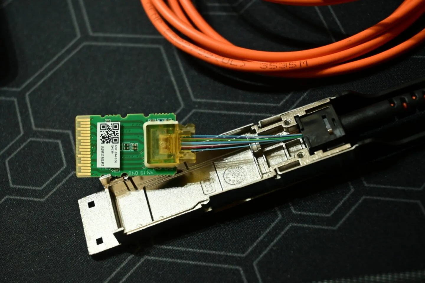
For context, Neon Control previously reported on programmable optics tested for AI networks, a separate approach to optical interconnects. The accompanying photo shows a disassembled 40 Gb/s QSFP transceiver for context; it is not a USFP prototype.